• Greeting
    • EMC Lab
    • Environment
    • Awards & Honors
    • Contact&Map
    • 3DIC
    • Near-Field Magnetic Probe
    • Signal Integrity
    • Electromagnetic and radio frequency interference (EMI & RFI)
    • Power Integrity
    • Microwave Circuits
    • Postdoctoral Research Fellow
    • Professor
      • CV
      • Introduction
    • Ph.D Students
    • Master Students
    • Assistants
    • Graduated Students
    • Exchange Student
    • Journal
    • Conference
    • Industry
    • Government
    • Electromagnetic Compatibility
    • Electromagnetics II
    • Microwave Filter Design
    • RF Microwave Systems
    • Complex Variables
Research
  • Signal Integrity
  • Near-Field Magnetic Probe
  • 3DIC
  • Electromagnetic and radio frequency interference (EMI & RFI)
  • Power Integrity
  • Microwave Circuits
Electro Magnetic Compatibility » Research » Power Integrity » Power Integrity on PCB, Package, and Chip Level

Power Integrity on PCB, Package, and Chip Level

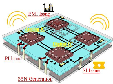
Power distribution network (PDN) design has became one of the major concerns in designing high-speed circuits or mixed signal systems in recent few years. The challenge is expected to increase in next decade as electronic systems are driven in the direction of faster digital speed, higher integration with radio frequency circuits, and higher throughput of data communication.

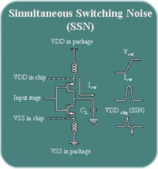
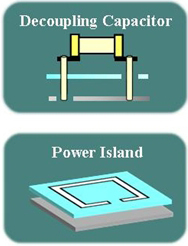
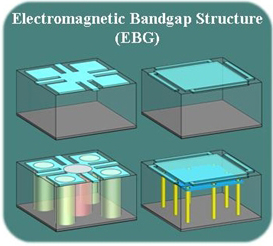
  We are interesting in both the formation mechanism and isolation design of the power noise. However, several solutions, such as decoupling capacitors and power island, for maintaining the power integrity are not sufficient enough. In particular, the electromagnetic bandgap (EBG) technology, which we are also focused on, provides a promising solution to significantly reduce the noise propagation through power distribution network.

Visitors :
Electro Magnetic Compatibility Lab. 版權所有 2025 © All rights reserved
網頁設計 by:奈思網頁設計公司